What is Trinita® ?
Trinita®とは
Trinita® is a single-stage RISC-V (RV32IM) IP core that connects instruction memory directly to the decoder — completing every instruction in exactly one clock cycle. No pipeline. No branch prediction. No hazards. Drop it into your FPGA today.
Trinita®は命令メモリをデコーダに直結し、すべての命令を1クロックで完結させるIPコアです。パイプラインを持たないシンプルな設計により、分岐予測もハザード処理も不要。RISC-V(RV32IM)準拠で、FPGAへの実装がすぐに始められます。
Note: The current model is also capable of being implemented in RISC-V(RV64IM).
注記:RISC-V(RV64IM)にも対応可能です。
What Hazard-Free Trinita® Solves
"Low power and deterministic real-time execution — at the same time." Trinita® delivers both.
6.4%
Energy vs.
MicroBlaze™
MicroBlaze™
1/2.5×
Clock freq. for
equal throughput
equal throughput
2+ days
SpO2 monitoring
on one AA battery
on one AA battery
| Trinita® | 5-stage Pipeline (MicroBlaze™ equiv.) | |
|---|---|---|
| Energy (Dhrystone) | 0.224 J | 3.488 J |
| Operating frequency | 1/2.5× for equal throughput | baseline |
| Hazard Occurrence | No | Yes |
| Clock Count (Branch/Interrupt) | ◎ Fully deterministic | △ Variable |
*Dhrystone benchmark v2.2, 512,000 iterations / Arty-A7 100T / 25MHz
Source:
*K.Hatakeyama et al., “An “Energy Efficient Processor Applicable to Continuous SPO2 Monitoring (https://ieeexplore.ieee.org/document/9621795),” in Proceedings of 2021 IEEE 10th Global Conference on Consumer Electronics (GCCE), 2021.
Note:
*The current model further halves energy consumption.
*Proven in a pulse oximeter: continuous SpO2 monitoring for 2+ days on a single AA rechargeable battery. Try the free evaluation build on GitHub — runs on Efinix® Sapphire SoC today.
ハザードレスなTrinita®が解決すること
「低消費電力と確定的なリアルタイム動作を、同時に実現したい」——その要求に正面から応えます。
6.4%
MicroBlaze™比の
エネルギー消費量(J)
エネルギー消費量(J)
1/2.5
同等処理に必要な
動作周波数
動作周波数
2日+
単三電池1本で
SpO2連続稼働
SpO2連続稼働
| Trinita® | MicroBlaze™(5ステージパイプライン) | |
|---|---|---|
| 消費電力量(Dhrystone) | 0.224 J | 3.488 J |
| 動作周波数 | 同等処理を 1/2.5× で実現 | 基準 |
| ハザードの発生 | なし | あり |
| 条件分岐や割り込み処理に要するクロック数 | ◎ 確定的 | △ 不確定 |
*Dhrystone benchmark v2.2、512,000回実行 / Arty-A7 100T / 25MHz
出典:
*K.Hatakeyama他、「An Energy Efficient Processor Applicable to Continuous SPO2 Monitoring」、GCCE 2021論文集
注記:
*現在はTrinnitaⓇの性能向上により、エネルギー消費量(J)はさらに半減しています。
*充電式単三電池1本でSpO2の2日以上連続モニタリングを実証済み。IoTセンサ・ヘルスケア・エッジAIへの組み込みに、まずは評価版をお試しください。
Topics / トピックス
🆕 Now Available on GitHub — Trinita® 1-Stage RISC-V Core Efinix® Trion™ T8 / T20 / Titanium™ Ti60対応
GitHub公開中 — 評価版を今すぐ試せます ▶ Try Free Evaluation (GitHub) / 評価版を試す
Note: TrinitaⓇ is based on our patented architecture. It is also capable of being implemented in devices other than those mentioned above (including ASIC). For more information, please use our contact form.
注記:TrinitaⓇはアーキテクチャ特許のため、上記以外のデバイス(ASIC含む)への実装も可能です。詳細については、お問い合わせフォームをご利用ください。
Trinita® Features
Trinita® の特徴

No Instruction. No Fetch Stage.
Non‑pipeline, Single‑stage Architecture
命令の読み出し時間ゼロ。非パイプライン・1ステージ構成
Instruction memory connects directly to the decoder. No instruction register, no fetch stage. An instruction cycle is processed in one stage
(one clock) because of the simple design.
命令メモリをデコーダに直結。インストラクション・レジスタなし、フェッチステージなし。
ノイマンボトルネックを軽減する「命令の読み出し時間ゼロ」で1命令サイクルを1ステージ(1クロック)で処理します。
Note: Trinita® is designed with a Harvard architecture.
注記:Trinita®はハーバード型アーキテクチャで設計されています。

Zero Hazards. No Branch Prediction.
ハザードゼロ。分岐予測不要。
All instructions complete sequentially in one clock. Control hazards and data hazards cannot occur. Branch prediction logic is unnecessary by design.
すべての命令が1クロックで逐次完了するため、制御ハザードもデータハザードも原理的に発生しません。分岐予測ロジックは設計上不要です。

1/2.5 the Clock Frequency. Equivalent Throughput.
動作周波数1/2.5。同等のスループット。
Achieves the same throughput as a 5-stage pipeline at 1/2.5 the operating frequency. Lower frequency means lower dynamic power — without sacrificing performance.
5ステージパイプラインと同等のスループットを、1/2.5の動作周波数で実現。周波数を下げることで動的消費電力を削減しながら、性能を維持します。
*Compared with the 5-stage pipeline.
*5ステージパイプラインとの比較

Deterministic Execution — Fixed Clock Count per Task
確定的実行 — タスクあたりのクロック数が確定
Every instruction completes in exactly one clock. The number of clocks required for any task is fully predictable — simplifying real-time scheduling and enabling robust multi-core design.
すべての命令が厳密に1クロックで完結します。任意のタスクに要するクロック数が完全に予測可能なため、リアルタイムスケジューリングが
容易になり、堅牢なマルチコア設計が可能です。

0.224 J vs 3.488 J on FPGA — Verified on Silicon
0.224 J vs 3.488 J (FPGA実装時) — シリコンで実証済み
Dhrystone benchmark (v2.2, 512,000 iterations) on Arty-A7 100T at 25 MHz: Trinita® consumed 0.224 J versus 3.488 J for MicroBlaze™ — 6.4% of the 5-stage pipeline equivalent. ASIC prototypes fabricated in ROHM 180 nm and Renesas SOTB 65 nm.
*Based on collaborative research with Hirosaki University.
Source: K.Hatakeyama et al.,“An Energy Efficient Processor Applicable to…” 2021.
Note: The current model achieved higher performance, while successfully further halving energy consumption.
Arty-A7 100T / 25MHzでのDhrystoneベンチマーク(v2.2、512,000回):Trinita®は0.224J、MicroBlaze™は3.488J。5ステージパイプライン比6.4%を実測。ROHM 180nmおよびルネサス SOTB 65nmプロセスでのASIC試作も完了しています。
*弘前大学との共同研究による
出典:K.Hatakeyama他、「An Energy Efficient Processor Applicable to Continuous SPO2 Monitoring」、GCCE 2021論文集
注記:現在はTrinitaⓇの性能向上により、エネルギー消費量はさらに半減しています。
Use Cases
活用領域
Trinita® leverages its lightweight single‑stage architecture and compact footprint to support a wide range of applications—from ultra‑low‑power IoT devices to edge AI and even space‑related systems. Its simple and easy‑to‑handle architecture also makes it suitable for research, education, and control‑oriented systems, enabling flexible integration designed for real‑world deployment.
Trinita®は、軽量な 1 ステージ構成と小型フットプリントを活かし、超低消費電力が求められる IoT から、エッジAI、宇宙用途まで幅広い領域で活用できます。
シンプルで扱いやすいアーキテクチャは、研究・教育用途や制御系システムにも適しており、実環境での応用を前提とした柔軟な組み込みが可能です。

Ultra-low-power IoT Devices
超低消費電力 IoTデバイス
Proven in continuous sensor operation. Trinita®'s low clock frequency and single-stage design minimize dynamic power without sacrificing throughput — ideal for battery-powered nodes requiring always-on operation.
Verified applications:
Environmental sensors / Agricultural IoT / Industrial monitoring nodes / BLE beacons / Smart home devices
連続センサー動作で実証済み。低動作周波数と1ステージ設計により、スループットを維持しながら動的
消費電力を最小化。常時動作が求められるバッテリー駆動ノードに最適です。
実証済み用途:
温湿度・環境センサー / 農業IoT / 産業用モニタリングノード / BLEビーコン /
スマートホームデバイス

Wearable & Healthcare Devices
ウェアラブル・ヘルスケア機器
Demonstrated in continuous SpO2 monitoring for 2+ days on a single AA rechargeable battery. Deterministic execution enables reliable real-time vital-sign processing in compact, low-power form factors.
Source: K.Hatakeyama et al., “An Energy Efficient Processor Applicable to…”2021.
Note: The current model enables 2x longer monitoring.
Verified applications:
SpO2 monitoring / Fitness trackers / Heart rate & temperature monitors /
Medical patch sensors
充電式単三電池1本でSpO2を2日以上連続モニタリングすることを実証済み。確定的実行により、小型・
低消費電力の筐体でも信頼性の高いリアルタイムバイタルサイン処理が可能です。
出典:Hatakeyama他、「An Energy Efficient Processor Applicable to Continuous SPO2 Monitoring」、
GCCE 2021論文集
注記:現在はTrinita®の性能向上により、さらに2倍の時間のモニタリングが可能です。
実証済み用途:
SpO2モニタリング / フィットネストラッカー / 心拍・体温モニタ /
医療用パッチセンサー

Edge AI — Lightweight Inference
エッジAI — 超軽量推論
AI and image processing edge computing is documented in official materials, supported by Trinita®'s robust multi-core capability and deterministic execution.
Verified applications: AI and image processing edge computing
Potential applications:
Anomaly detection (vibration/sound/motor) / Keyword spotting / Simple gesture recognition / Low-resolution object detection / On-device training and inference
AI・画像処理のエッジコンピューティングは公式資料に記載済み。Trinita®の堅牢なマルチコア性能と確定的実行がこれを支えます。
実証済み用途: AI・画像処理のエッジコンピューティング
展開想定:
異常検知(振動・音・モーター) / キーワードスポッティング / 簡易ジェスチャー認識 / 低解像度物体検知 / オンデバイス学習・推論

Edge Control — Motors, Robotics & Industrial
エッジ制御 — モーター・ロボティクス・産業機器
Deterministic clock-per-instruction execution and robust multi-core operation are documented in official materials, maintaining real-time performance and power efficiency even as branch and interrupt frequency increases.
Verified applications: Systems requiring real-time performance
Potential applications: Motor control, robotics, and other timing-critical domains
1命令1クロックの確定的実行と堅牢なマルチコア動作は公式資料に記載済み。
分岐・割り込み頻度が上がってもリアルタイム性と電力効率を維持します。
実証済み用途:リアルタイム性が求められるシステム全般
展開想定: モーター制御・ロボティクスなど、タイミング保証が重要な分野

Education & Research — RISC-V Implementation
教育・研究 — RISC-V実装学習
A free evaluation build is publicly available on GitHub, ready to run on Efinix® Trion® and Titanium® FPGAs. Trinita®'s single-stage simplicity makes it an ideal reference design for CPU architecture courses and SoC design exercises.
Verified applications:
CPU architecture courses / SoC design exercises / FPGA implementation experiments / Lightweight research prototypes
無償評価版をGitHubで公開中。Efinix® Trion®およびTitanium® FPGAですぐに動作確認できます。
1ステージ設計のシンプルさは、CPUアーキテクチャの授業やSoC設計演習のリファレンス実装として
最適です。
実証済み用途:
CPUアーキテクチャ授業 / SoC設計演習 / FPGA実装実験 /
研究用軽量プロトタイプ
Looking Ahead
将来の可能性

Space & Satellite Computing
宇宙・衛星向けコンピューティング
Trinita®'s fully deterministic execution and ultra-low power consumption are architectural characteristics with potential relevance to space applications, such as satellite attitude control and telemetry processing. This is an exploratory direction — not yet evaluated or verified for space environments (including radiation tolerance).
Potential applications: CubeSat attitude control / Telemetry processing
*Exploratory — Future Direction
Trinita®の完全な確定的実行と超低消費電力という特性は、衛星の姿勢制御やテレメトリ処理といった宇宙用途にも理論上関連する可能性があります。これは構想段階の可能性であり、宇宙環境(放射線耐性を含む)での評価・検証は行われていません。
展開想定: 小型衛星(CubeSat)の姿勢制御 / テレメトリ処理
*構想段階 — 将来の方向性
Architecture Overview
アーキテクチャ概要
Trinita® eliminates the instruction fetch stage entirely by connecting instruction memory (RAM) directly to the decoder — removing the instruction register and completing every instruction in exactly one clock cycle.
In a conventional 5-stage pipeline, conditional branches and interrupts cause pipeline flushes and stalls. Trinita®'s single-stage design has no pipeline, so no control hazards or data hazards can occur. Branch prediction logic is unnecessary by design.
Because all instructions complete in one clock, the number of clocks required for any given task is fully deterministic — a property that makes real-time scheduling straightforward and enables robust multi-core implementation without sacrificing throughput.
Operating at 1/2.5 the clock frequency of a 5-stage pipeline while delivering equivalent throughput, Trinita® achieves dramatically lower dynamic power. Verified on Xilinx® Artix®-7 100T (25 MHz): energy consumption during Dhrystone execution (512,000 iterations) measures 0.224 J versus 3.488 J for Xilinx® MicroBlaze™ — 6.4% of the pipeline equivalent.
Source: K.Hatakeyama et al., “An Energy Efficient Processor Applicable to…”2021.
Note: The current model further halves energy consumption.
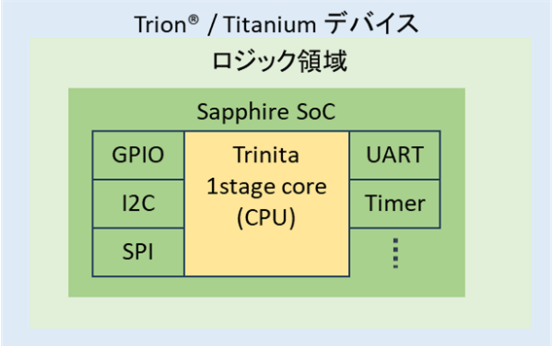
The core is implemented in Verilog and integrates into Efinix® Sapphire SoC as a drop-in replacement for the VexRiscv core. FPGA targets include all EfinixⓇ FPGAs (TrionⓇ / Titanium™ / Topaz™).
Proprietary peripherals available. ASIC prototypes have been fabricated in ROHM 180 nm and Renesas SOTB 65 nm processes in joint research with Hirosaki University.
Note: TrinitaⓇ is based on our patented architecture. It is also capable of being implemented in devices other than those mentioned above (including ASIC). For more information, please use our contact form.
Trinita®は、命令メモリ(RAM)をデコーダに直結することで命令フェッチステージを完全に排除し、インストラクション・レジスタを不要とします。すべての命令を1クロックで完結させる、
極めてシンプルな設計です。
通常の5ステージパイプラインでは、条件分岐や割込み発生時にパイプラインのフラッシュやストールが生じます。Trinita®はパイプラインを持たないため、制御ハザードもデータハザードも原理的に発生せず、
分岐予測ロジックも不要です。
すべての命令が1クロックで逐次完了するため、任意の処理に要するクロック数は完全に確定的です。これによりリアルタイムスケジューリングが容易になるとともに、スループットを損なわない堅牢なマルチコア化が可能になります。
5ステージパイプラインの約1/2.5の動作周波数で同等の処理量を実現するため、動的消費電力を大幅に削減できます。Xilinx® Artix®-7 100T(25MHz)での実測値:Dhrystoneベンチマーク512,000回実行時の
エネルギー消費量は0.224J(Xilinx® MicroBlaze™は3.488J)、すなわちパイプライン比6.4%を実証済みです。
出典:K.Hatakeyama他、「An Energy Efficient Processor Applicable to Continuous SPO2 Monitoring」、GCCE 2021論文集
注記:現在はTrinitaⓇの性能向上により、エネルギー消費量(J)はさらに半減しています。
コアはVerilogで実装され、Efinix® Sapphire SoCにVexRiscvコアの差し替えとして統合できます。全てのEfinixⓇ FPGAs (TrionⓇ / Titanium™ / Topaz™)に対応可能です。また、当社独自のペリフェラルのご用意もあります。ASICについては弘前大学との共同研究によりROHM 180nmおよびルネサスエレクトロニクス SOTB 65nmプロセスでの試作を完了しています。
注記:Trinita®はアーキテクチャ特許のため、上記以外のデバイス(ASIC含む)への実装も可能です。詳しくは「コンタクト」からお問い合わせください。
Instruction Flow Comparison(1‑Stage vs 5‑Stage)
命令処理フローの比較(1ステージ vs 5ステージ)
The 5-stage pipeline introduces stalls on every branch and interrupt.
The 1-stage design has none — every instruction completes in one clock, every time.
(Click image to expand)
5ステージパイプラインは分岐・割り込みのたびにストールが発生します。
1ステージ設計にストールはなく、すべての命令が常に1クロックで完結します。
※画像をクリックすると拡大します
Specifications/仕様一覧 (for Efinix® FPGAs)
Note: For implementation in third-party FPGAs, please contact us.
注記: 他社FPGAsへの実装はご相談ください。
(Click image to expand)
※画像をクリックすると拡大します。
| Item / 項目 | Specification / 内容 |
|---|---|
| Architecture / アーキテクチャ | 1-Stage (Single-Cycle, Non-pipeline) 1ステージ(1命令サイクル、非パイプライン) |
| ISA/ 命令セット | RISC-V RV32IM* *Also available for RISC-V RV64IM. *RISC-V RV64IMにも対応可。 |
| Performance / 性能 (No Cache / キャッシュなし) | 1.79 DMIPS/MHz 2.9 CoreMark/MHz ※ vs. VexRiscv(6-stage pipeline/6ステージパイプライン) 1.08 DMIPS/MHz ・1.69 CoreMark/MHz |
| Operating Frequency / 動作周波数 | Trion® T8: 13 MHz Trion® T20: 30 MHz Titanium™ Ti60: 83 MHz |
| On-chip Memory / オンチップメモリ |
T8: 8 KB (imem 4KB + dmem 4KB) T20: 64 KB (imem 32KB + dmem 32KB) Ti60: 64 KB (imem 32KB + dmem 32KB) *For alternative memory sizes, please contact us. *メモリ容量はご相談ください。 |
| CPU Register / CPUレジスタ | Selectable: Block RAM or FF Block RAM または FF(選択可) |
| Pipeline / パイプライン | None — Hazard-free, no branch prediction required 分岐予測・ハザード処理不要。 |
| Supported Boards / 対応ボード |
All Efinix® development kits すべてのEfinix®開発キット |
| Target Device / ターゲット | All Efinix®FPGAs(Trion®/Titanium™/Topaz™) すべてのEfinix®FPGAs *Can replace VexRiscv-Core of Efinix® Sapphire SoC *Efinix® Sapphire SoC(VexRiscvコアと差し替え可) |
| Peripherals / ペリフェラル |
Proprietary Peripherals:UART x 2ch, I2C x 2ch, SPI x 2ch *One channel (1ch) each is available for T8. *Existing peripherals of Efinix® Sapphire SoC can be reused as-is during core replacement. *For customization such as adding or modifying features, please contact us. 当社独自のペリフェラル:UART x 2ch, I2C x 2ch, SPI x 2ch *T8は各1chずつ使用可能。 *コア差し替え時はEfinix® Sapphire SoCのペリフェラルをそのまま使用可能。 *機能追加・変更等のカスタマイズについてはご相談ください。 |
| HDL / 設計言語 | Verilog |
| EDA Tool / 開発環境 | Efinity® IDE 2023.2 or later / RISC-V IDE 2023.1 or later Efinity® IDE 2023.2以降 / RISC-V IDE 2023.1以降 |
| Patent / 特許 |
US 8,516,225 B2 / US 12,111,788 B2 JP 4862100 / JP 7384374 TW I-389027 / TW I-862545 KR 10-1178293 |
| License / ライセンス | Free evaluation build available (1-hour limit) Commercial license available 無償評価版あり(動作時間1時間制限)。 商用ライセンス:お問い合わせください。 |
*Performance figures are based on internal testing and may vary depending on implementation conditions.
*Please contact us for ASIC conversion inquiries.
*性能数値は当社比(実装条件により変動します)。
*ASIC化をご検討の場合はご相談ください。
Integration Examples
組み込み例
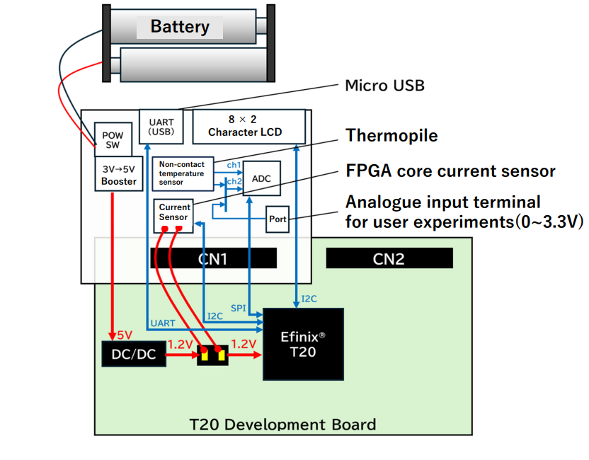
FPGA Integration — Trion® T20 Non-contact Thermometer Demo
FPGA組み込み例 — Trion® T20 非接触温度計デモ
PDF:
https://www.unolabo.co.jp/s/Trion_T20-demo.pdf
(English)
https://www.unolabo.co.jp/s/demo_Trion_T20_.pdf
(日本語)
Trinita® 1-stage RISC-V core implemented on Efinix® Trion® T20, demonstrated in a battery-powered non-contact thermometer. Operating at 25 MHz, Trinita® delivers equivalent throughput to Sapphire SoC (VexRiscv) at 42 MHz while consuming 44.6 mW versus 71.2 mW — a 37% power reduction. In applications with frequent branch instructions and interrupts, the advantage of Trinita®'s hazard-free design widens further.
Efinix® Trion® T20にTrinita® 1ステージ RISC-Vコアを実装し、バッテリー駆動の非接触温度計として動作実証しました。25MHz動作でSapphire SoC(VexRiscv)の42MHz動作と同等の処理量を実現しながら、消費電力は44.6mW対71.2mWと37%削減。条件分岐や割り込みが多い負荷の高いプログラムでは、処理遅延のないTrinita®のメリットがさらに広がります。
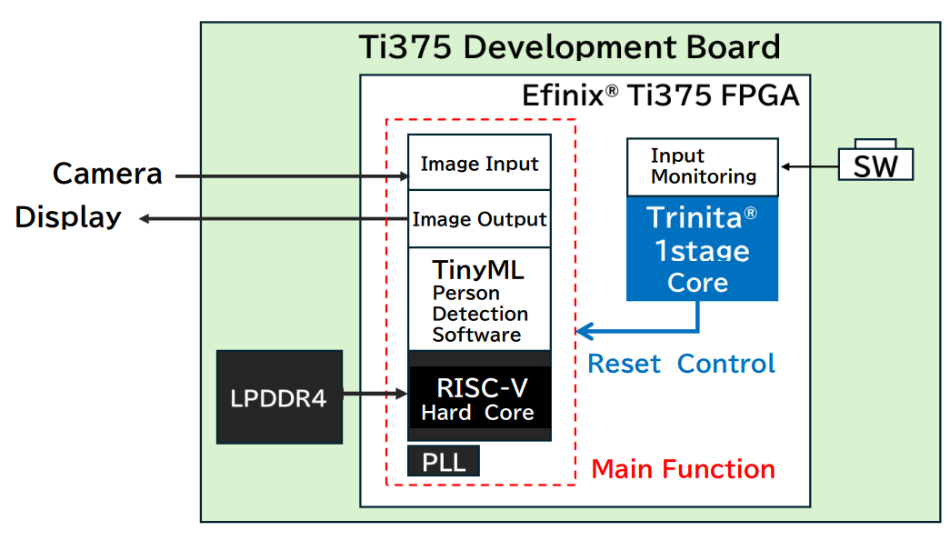
SoC Integration — Trinita® as Subsystem in Titanium™ Ti375
SoC組み込み例 — Titanium™ Ti375 サブシステムとしての実装
PDF:
https://www.unolabo.co.jp/s/Titanium_Ti375Trinita.pdf
(Japanese language only / 日本語のみ)
Trinita® 1-stage RISC-V core (RV32IM) implemented as a subsystem within Efinix® Titanium™ Ti375C529 FPGA, which features a quad-core hardened RISC-V block. The implementation uses 6,831 of 362,880 available logic elements — allowing up to 53 Trinita® cores to be instantiated simultaneously in the logic area. Peripherals include SPI×1, I2C×2, UART×2, and GPIO.
クアッドコアハードRISC-Vブロックを搭載したEfinix® Titanium™ Ti375C529 FPGAのサブシステムとしてTrinita® 1ステージ RISC-Vコア(RV32IM)を実装しました。使用ロジック数は362,880中6,831で、ロジック領域に理論上最大53セットの同時実装が可能です。ペリフェラルはSPI×1、I2C×2、UART×2、GPIOをサポートします。
System Demo — Trinita® Sleep Control in Titanium™ Ti375
システム構成例 — Titanium™ Ti375 スリープ制御デモ
PDF:
https://www.unolabo.co.jp/s/Titanium_Ti375-demo.pdf (English)
https://www.unolabo.co.jp/s/demo_Titanium_Ti375Trinita.pdf (日本語)
A real-world system demo implementing Trinita® 1-stage RISC-V core (RV32IM) as a subsystem in Efinix® Titanium™ Ti375C529 FPGA, demonstrating low-power sleep control for an event venue crowd monitoring system. Trinita® remains active during sleep mode to monitor inputs, enabling instant wake-up. Operating at 25 MHz, it matches VexRiscv at 42 MHz in throughput while achieving lower power consumption.
The demo also demonstrates robust multi-core scaling — with no hazards or wasted cycles, real-time performance and power efficiency are maintained even as branch and interrupt frequency increases.
Efinix® Titanium™ Ti375C529 FPGAのサブシステムとしてTrinita® 1ステージ RISC-Vコア(RV32IM)を実装し、イベント会場の混雑状況リアルタイム表示システムでの低消費電力スリープ制御を実証しました。スリープ中もTrinita®が動作して入力を監視し、ボタン押下で即座にメイン機能が復帰します。25MHz動作でVexRiscv 42MHz相当の処理量を実現しながら低消費電力を達成。ハザードや無駄な処理が発生しないため、分岐・割り込み頻度が上がっても高いリアルタイム性と電力効率を維持したまま堅牢なマルチコア分散処理が可能です。
Integration Examples
組み込み例
FPGA Integration — Trion® T20 Non-contact Thermometer Demo
FPGA組み込み例 — Trion® T20 非接触温度計デモ
PDF: https://www.unolabo.co.jp/s/Trion_T20-demo.pdf (English)
https://www.unolabo.co.jp/s/demo_Trion_T20_.pdf (日本語)
Trinita® 1-stage RISC-V core implemented on Efinix® Trion® T20, demonstrated in a battery-powered non-contact thermometer. Operating at 25 MHz, Trinita® delivers equivalent throughput to Sapphire SoC (VexRiscv) at 42 MHz while consuming 44.6 mW versus 71.2 mW — a 37% power reduction. In applications with frequent branch instructions and interrupts, the advantage of Trinita®'s hazard-free design widens further.
Efinix® Trion® T20にTrinita® 1ステージ RISC-Vコアを実装し、バッテリー駆動の非接触温度計として動作実証しました。25MHz動作でSapphire SoC(VexRiscv)の42MHz動作と同等の処理量を実現しながら、消費電力は44.6mW対71.2mWと37%削減。条件分岐や割り込みが多い負荷の高いプログラムでは、処理遅延のないTrinita®のメリットがさらに広がります。
SoC Integration — Trinita® as Subsystem in Titanium™ Ti375
SoC組み込み例 — Titanium™ Ti375 サブシステムとしての実装
PDF: https://www.unolabo.co.jp/s/Titanium_Ti375Trinita.pdf (Japanese language only / 日本語のみ)
Trinita® 1-stage RISC-V core (RV32IM) implemented as a subsystem within Efinix® Titanium™ Ti375C529 FPGA, which features a quad-core hardened RISC-V block. The implementation uses 6,831 of 362,880 available logic elements — allowing up to 53 Trinita® cores to be instantiated simultaneously in the logic area. Peripherals include SPI×1, I2C×2, UART×2, and GPIO.
クアッドコアハードRISC-Vブロックを搭載したEfinix® Titanium™ Ti375C529 FPGAのサブシステムとしてTrinita® 1ステージ RISC-Vコア(RV32IM)を実装しました。使用ロジック数は362,880中6,831で、ロジック領域に理論上最大53セットの同時実装が可能です。ペリフェラルはSPI×1、I2C×2、UART×2、GPIOをサポートします。
System Demo — Trinita® Sleep Control in Titanium™ Ti375
システム構成例 — Titanium™ Ti375 スリープ制御デモ
PDF: https://www.unolabo.co.jp/s/Titanium_Ti375-demo.pdf (English)
https://www.unolabo.co.jp/s/demo_Titanium_Ti375Trinita.pdf (日本語)
A real-world system demo implementing Trinita® 1-stage RISC-V core (RV32IM) as a subsystem in Efinix® Titanium™ Ti375C529 FPGA, demonstrating low-power sleep control for an event venue crowd monitoring system. Trinita® remains active during sleep mode to monitor inputs, enabling instant wake-up. Operating at 25 MHz, it matches VexRiscv at 42 MHz in throughput while achieving lower power consumption.
The demo also demonstrates robust multi-core scaling — with no hazards or wasted cycles, real-time performance and power efficiency are maintained even as branch and interrupt frequency increases.
Efinix® Titanium™ Ti375C529 FPGAのサブシステムとしてTrinita® 1ステージ RISC-Vコア(RV32IM)を実装し、イベント会場の混雑状況リアルタイム表示システムでの低消費電力スリープ制御を実証しました。スリープ中もTrinita®が動作して入力を監視し、ボタン押下で即座にメイン機能が復帰します。25MHz動作でVexRiscv 42MHz相当の処理量を実現しながら低消費電力を達成。ハザードや無駄な処理が発生しないため、分岐・割り込み頻度が上がっても高いリアルタイム性と電力効率を維持したまま堅牢なマルチコア分散処理が可能です。
Trusted by Research. Proven in Silicon.
研究機関と歩み、シリコンで証明された技術力
Trinita® is not a concept — it is a production-ready IP core backed by peer-reviewed research, international patents, and silicon-proven results.
構想から実装へ。Trinita®は査読済み論文・国際特許・シリコン実証済みの結果に裏付けられた、実用レベルのIPコアです。
Joint Research / 共同研究 Hirosaki University — Since 2018 / 弘前大学 — 2018年より
Peer-Reviewed Papers / 査読済み論文 IEEE MWSCAS 2019 / IEEE GCCE 2021 / SASIMI 2021 / SASIMI 2024
Silicon-Proven / シリコン実証済み ROHM 180nm ASIC / Renesas SOTB 65nm ASIC
International Patents / 国際特許(7件) US 8,516,225 B2 / US 12,111,788 B2 / JP 4862100 / JP 7384374 / TW I-389027 / TW I-862545 / KR 10-1178293
Official Partner / 公式パートナー認定 Efinix® Official Partner — Asia Pacific
RISC-V International Strategic Member
Award / 受賞 Innovation Business Award 2021 "Yoi Shigoto Okoshi Award" / よい仕事おこし賞 (Sponsored by Johnan Shinkin Bank / 城南信用金庫提供)
Contact / お問い合わせ
For commercial licensing, technical questions, or partnership inquiries, please reach out.
商用ライセンス・技術的なご質問・ パートナーシップについては お気軽にお問い合わせください。
Use Cases
活用領域
Ultra-low-power IoT Devices
超低消費電力 IoTデバイス
Proven in continuous sensor operation. Trinita®'s low clock frequency and single-stage design minimize dynamic power without sacrificing throughput — ideal for battery-powered nodes requiring always-on operation.
Verified applications:
Environmental sensors / Agricultural IoT / Industrial monitoring nodes / BLE beacons / Smart home devices
連続センサー動作で実証済み。低動作周波数と1ステージ設計により、スループットを維持しながら動的
消費電力を最小化。常時動作が求められるバッテリー駆動ノードに最適です。
実証済み用途:
温湿度・環境センサー / 農業IoT / 産業用モニタリングノード / BLEビーコン /
スマートホームデバイス
Wearable & Healthcare Devices
ウェアラブル・ヘルスケア機器
Demonstrated in continuous SpO2 monitoring for 2+ days on a single AA rechargeable battery. Deterministic execution enables reliable real-time vital-sign processing in compact, low-power form factors.
Source: K.Hatakeyama et al., “An Energy Efficient Processor Applicable to…”2021.
Note: The current model enables 2x longer monitoring.
Verified applications:
SpO2 monitoring / Fitness trackers / Heart rate & temperature monitors /
Medical patch sensors
充電式単三電池1本でSpO2を2日以上連続モニタリングすることを実証済み。確定的実行により、小型・
低消費電力の筐体でも信頼性の高いリアルタイムバイタルサイン処理が可能です。
出典:Hatakeyama他、「An Energy Efficient Processor Applicable to Continuous SPO2 Monitoring」、
GCCE 2021論文集
注記:現在はTrinita®の性能向上により、さらに2倍の時間のモニタリングが可能です。
実証済み用途:
SpO2モニタリング / フィットネストラッカー / 心拍・体温モニタ /
医療用パッチセンサー
Edge AI — Lightweight Inference
エッジAI — 超軽量推論
AI and image processing edge computing is documented in official materials, supported by Trinita®'s robust multi-core capability and deterministic execution.
Verified applications: AI and image processing edge computing
Potential applications:
Anomaly detection (vibration/sound/motor) / Keyword spotting / Simple gesture recognition / Low-resolution object detection / On-device training and inference
AI・画像処理のエッジコンピューティングは公式資料に記載済み。Trinita®の堅牢なマルチコア性能と確定的実行がこれを支えます。
実証済み用途: AI・画像処理のエッジコンピューティング
展開想定:
異常検知(振動・音・モーター) / キーワードスポッティング / 簡易ジェスチャー認識 / 低解像度物体検知 / オンデバイス学習・推論
Edge Control — Motors, Robotics & Industrial
エッジ制御 — モーター・ロボティクス・産業機器
Deterministic clock-per-instruction execution and robust multi-core operation are documented in official materials, maintaining real-time performance and power efficiency even as branch and interrupt frequency increases.
Verified applications: Systems requiring real-time performance
Potential applications: Motor control, robotics, and other timing-critical domains
1命令1クロックの確定的実行と堅牢なマルチコア動作は公式資料に記載済み。
分岐・割り込み頻度が上がってもリアルタイム性と電力効率を維持します。
実証済み用途:リアルタイム性が求められるシステム全般
展開想定: モーター制御・ロボティクスなど、タイミング保証が重要な分野
Education & Research — RISC-V Implementation
教育・研究 — RISC-V実装学習
A free evaluation build is publicly available on GitHub, ready to run on Efinix® Trion® and Titanium® FPGAs. Trinita®'s single-stage simplicity makes it an ideal reference design for CPU architecture courses and SoC design exercises.
Verified applications:
CPU architecture courses / SoC design exercises / FPGA implementation experiments / Lightweight research prototypes
無償評価版をGitHubで公開中。Efinix® Trion®およびTitanium® FPGAですぐに動作確認できます。
1ステージ設計のシンプルさは、CPUアーキテクチャの授業やSoC設計演習のリファレンス実装として
最適です。
実証済み用途:
CPUアーキテクチャ授業 / SoC設計演習 / FPGA実装実験 /
研究用軽量プロトタイプ